- 您现在的位置:买卖IC网 > Sheet目录3886 > PIC16C54C-04/SO (Microchip Technology)IC MCU OTP 512X12 18SOIC
2002 Microchip Technology Inc.
Preliminary
DS30453D-page 33
PIC16C5X
6.7
Indirect Data Addressing; INDF
and FSR Registers
The INDF Register is not a physical register.
Addressing INDF actually addresses the register
whose address is contained in the FSR Register (FSR
is a
pointer). This is indirect addressing.
EXAMPLE 6-1:
INDIRECT ADDRESSING
Register file 08 contains the value 10h
Register file 09 contains the value 0Ah
Load the value 08 into the FSR Register
A read of the INDF Register will return the value
of 10h
Increment the value of the FSR Register by one
(FSR = 09h)
A read of the INDF register now will return the
value of 0Ah.
Reading INDF itself indirectly (FSR = 0) will produce
00h. Writing to the INDF Register indirectly results in a
no-operation (although STATUS bits may be affected).
A simple program to clear RAM locations 10h-1Fh
using indirect addressing is shown in Example 6-2.
EXAMPLE 6-2:
HOW TO CLEAR RAM
USING INDIRECT
ADDRESSING
MOVLW
H’10’
;initialize pointer
MOVWF
FSR
; to RAM
NEXT
CLRF
INDF
;clear INDF Register
INCF
FSR,F
;inc pointer
BTFSC
FSR,4
;all done?
GOTO
NEXT
;NO, clear next
CONTINUE
:
;YES, continue
The FSR is either a 5-bit (PIC16C54, PIC16CR54,
PIC16C55,
PIC16C56,
PIC16CR56)
or
7-bit
(PIC16C57, PIC16CR57, PIC16C58, PIC16CR58)
wide register. It is used in conjunction with the INDF
Register to indirectly address the data memory area.
The FSR<4:0> bits are used to select data memory
addresses 00h to 1Fh.
PIC16C54,
PIC16CR54,
PIC16C55,
PIC16C56,
PIC16CR56: These do not use banking. FSR<6:5> bits
are unimplemented and read as '1's.
PIC16C57,
PIC16CR57,
PIC16C58,
PIC16CR58:
FSR<6:5> are the bank select bits and are used to
select the bank to be addressed (00 = bank 0,
01
=bank 1, 10 = bank 2, 11 = bank 3).
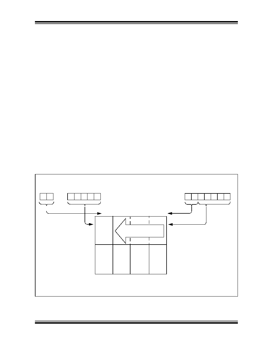
FIGURE 6-10:
DIRECT/INDIRECT ADDRESSING
Note
1: For register map detail see Section 6.2.
bank
location select
bank select
Indirect Addressing
Direct Addressing
Data
Memory(1)
0Fh
10h
Bank 0
Bank 1
Bank 2
Bank 3
0
4
5
6
(FSR)
10
00
01
11
00h
1Fh
3Fh
5Fh
7Fh
(opcode)
0
4
5
6
(FSR)
Addresses map back to
addresses in Bank 0.
3
2
1
3
2
1
发布紧急采购,3分钟左右您将得到回复。
相关PDF资料
PIC16F722-I/ML
IC PIC MCU FLASH 2KX14 28-QFN
PIC16LCE623T-04I/SO
IC MCU CMOS.5K OTP W/EEPRM18SOIC
PIC16HV540-04I/SO
IC MCU OTP 512X12 18SOIC
PIC16LCE623T-04E/SS
IC MCU CMOS.5K OTP W/EEPRM20SSOP
PIC16LCE623T-04E/SO
IC MCU CMOS.5K OTP W/EEPRM18SOIC
5-520415-4
CONN TRIOMATE 4POS VERT TIN
6-176982-6
CONN TRIO-MATE 16POS .100 FFC
PIC16LCE623-04I/SO
IC MCU CMOS.5K OTP W/EEPRM18SOIC
相关代理商/技术参数
PIC16C54C-04/SO
制造商:Microchip Technology Inc 功能描述:8BIT CMOS MCU SMD 16C54 SOIC18
PIC16C54C-04/SO
制造商:Microchip Technology Inc 功能描述:Microcontroller IC Number of I/Os:12
PIC16C54C-04/SS
功能描述:8位微控制器 -MCU .75KB 25 RAM 12 I/O 4MHz SSOP20 RoHS:否 制造商:Silicon Labs 核心:8051 处理器系列:C8051F39x 数据总线宽度:8 bit 最大时钟频率:50 MHz 程序存储器大小:16 KB 数据 RAM 大小:1 KB 片上 ADC:Yes 工作电源电压:1.8 V to 3.6 V 工作温度范围:- 40 C to + 105 C 封装 / 箱体:QFN-20 安装风格:SMD/SMT
PIC16C54C-04E/P
功能描述:8位微控制器 -MCU .75KB 25 RAM 12 I/O 4MHz ExtTemp PDIP18 RoHS:否 制造商:Silicon Labs 核心:8051 处理器系列:C8051F39x 数据总线宽度:8 bit 最大时钟频率:50 MHz 程序存储器大小:16 KB 数据 RAM 大小:1 KB 片上 ADC:Yes 工作电源电压:1.8 V to 3.6 V 工作温度范围:- 40 C to + 105 C 封装 / 箱体:QFN-20 安装风格:SMD/SMT
PIC16C54C-04E/SO
功能描述:8位微控制器 -MCU .75KB 25 RAM 12 I/O 4MHz Ext Temp SOIC18 RoHS:否 制造商:Silicon Labs 核心:8051 处理器系列:C8051F39x 数据总线宽度:8 bit 最大时钟频率:50 MHz 程序存储器大小:16 KB 数据 RAM 大小:1 KB 片上 ADC:Yes 工作电源电压:1.8 V to 3.6 V 工作温度范围:- 40 C to + 105 C 封装 / 箱体:QFN-20 安装风格:SMD/SMT
PIC16C54C-04E/SS
功能描述:8位微控制器 -MCU .75KB 25 RAM 12 I/O 4MHz Ext Temp SSOP20 RoHS:否 制造商:Silicon Labs 核心:8051 处理器系列:C8051F39x 数据总线宽度:8 bit 最大时钟频率:50 MHz 程序存储器大小:16 KB 数据 RAM 大小:1 KB 片上 ADC:Yes 工作电源电压:1.8 V to 3.6 V 工作温度范围:- 40 C to + 105 C 封装 / 箱体:QFN-20 安装风格:SMD/SMT
PIC16C54C-04I/P
功能描述:8位微控制器 -MCU .75KB 25 RAM 12 I/O 4MHz IndTemp PDIP18 RoHS:否 制造商:Silicon Labs 核心:8051 处理器系列:C8051F39x 数据总线宽度:8 bit 最大时钟频率:50 MHz 程序存储器大小:16 KB 数据 RAM 大小:1 KB 片上 ADC:Yes 工作电源电压:1.8 V to 3.6 V 工作温度范围:- 40 C to + 105 C 封装 / 箱体:QFN-20 安装风格:SMD/SMT
PIC16C54C-04I/P
制造商:Microchip Technology Inc 功能描述:IC 8BIT CMOS MCU 16C54 DIP18